
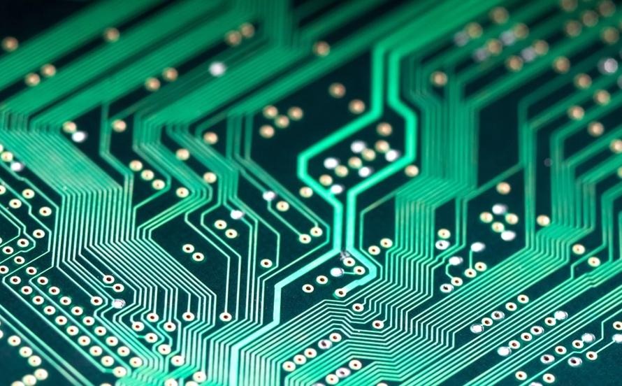
The rapid evolution of electronic technology has increased the demand for compact, lightweight, and high-performance circuit boards capable of supporting increasingly complex designs. From smartphones and medical equipment to automotive systems and telecommunications infrastructure, modern electronic products require greater functionality within smaller form factors. To meet these demands, manufacturers rely on the Multilayer PCB, one of the most advanced and widely used printed circuit board technologies available today.
Unlike single-sided or double-sided circuit boards, a multilayer PCB consists of multiple conductive copper layers separated by insulating dielectric materials and laminated into a single structure. This design enables engineers to create highly complex circuits while improving signal integrity, reducing electromagnetic interference, and maximizing component density. As a result, multilayer PCBs have become the preferred solution for sophisticated electronic products that require high reliability and outstanding electrical performance.
Producing multilayer circuit boards involves advanced manufacturing processes, precise layer alignment, and strict quality control. Choosing an experienced Multilayer PCB manufacturer is essential for ensuring reliable performance, manufacturing accuracy, and long-term product durability.
This article explains what a multilayer PCB is, how it is manufactured, its advantages, applications, and why selecting the right manufacturing partner is critical for modern electronics.
What Is a Multilayer PCB?
A Multilayer PCB is a printed circuit board that contains three or more conductive copper layers laminated together using insulating dielectric materials. These internal copper layers are interconnected through plated vias, allowing electrical signals and power to travel efficiently throughout the board.
The number of layers varies depending on circuit complexity and application requirements. Some electronic products may use four or six layers, while highly advanced communication systems, aerospace equipment, and servers may require more than twenty layers.
Each internal layer performs a specific function within the overall design. Certain layers are dedicated to signal routing, while others provide power distribution and grounding to improve electrical performance and minimize interference.
The multilayer construction enables engineers to develop compact electronic products with higher component density and more sophisticated functionality than would be possible using simpler PCB designs.
Why Multilayer PCBs Are Important
As electronic devices continue to shrink in size while increasing in functionality, efficient use of available circuit board space has become increasingly important. A Multilayer PCB allows designers to integrate complex electronic circuits into smaller products without compromising electrical performance.
Multiple internal layers improve signal routing by separating power, ground, and high-speed signal traces. This reduces electrical noise and electromagnetic interference while improving signal integrity for high-frequency applications.
The additional copper layers also enhance power distribution throughout the PCB, helping maintain stable voltage levels and improving overall system reliability. Better thermal management further supports high-performance electronic components that generate significant heat during operation.
These advantages make multilayer PCBs essential for modern electronic products requiring high-speed communication, advanced processing capabilities, and dependable long-term performance.
The Multilayer PCB Manufacturing Process
Manufacturing a Multilayer PCB begins with a detailed Design for Manufacturability (DFM) review. Engineers carefully evaluate the PCB stack-up, layer configuration, material selection, copper thickness, impedance control, thermal performance, and manufacturing tolerances before production starts.
The fabrication process begins by producing each individual circuit layer using precision photolithography and chemical etching. Once the copper patterns have been created, the individual layers are carefully aligned with insulating prepreg materials placed between them.
The complete layer stack is laminated under precisely controlled pressure and temperature to form a single rigid board. Accurate layer registration during this stage is essential because even slight misalignment can affect electrical performance.
Precision drilling creates vias that connect internal copper layers, followed by copper plating to establish reliable electrical connections throughout the PCB. Solder mask application protects exposed copper traces, while silkscreen printing provides assembly information before surface finishing improves solderability and corrosion resistance.
Every completed multilayer PCB undergoes comprehensive inspection and electrical testing before shipment to verify structural integrity and circuit functionality.
Advantages of Multilayer PCB Technology
One of the greatest advantages of a Multilayer PCB is its ability to accommodate highly complex electronic circuits within a compact footprint. Multiple conductive layers provide significantly greater routing capacity without increasing board size.
Improved electrical performance is another major benefit. Dedicated power and ground planes reduce electrical noise, improve signal integrity, and support stable high-speed communication between electronic components.
Multilayer PCBs also provide better mechanical strength because the laminated structure creates a rigid and durable circuit board capable of withstanding vibration and mechanical stress.
Enhanced thermal performance is achieved through optimized copper distribution that helps dissipate heat generated by processors, power devices, and communication circuits.
The increased design flexibility allows engineers to integrate sophisticated electronic functions while reducing overall product size, making multilayer PCBs indispensable for advanced electronic systems.
Applications of Multilayer PCBs
Multilayer PCBs are widely used across industries that require compact, high-performance electronic systems. Consumer electronics manufacturers rely on these circuit boards in smartphones, tablets, laptops, gaming consoles, wearable devices, and smart home products where high component density is essential.
Automotive manufacturers use multilayer PCBs in engine control units, battery management systems, advanced driver assistance systems, infotainment platforms, electric vehicle controllers, and autonomous driving technologies.
Telecommunications infrastructure incorporates multilayer PCBs into networking equipment, routers, communication switches, optical transmission systems, data centers, and 5G base stations that require high-speed signal transmission.
Medical equipment manufacturers depend on multilayer PCBs for diagnostic imaging systems, laboratory instruments, patient monitoring devices, surgical equipment, and portable healthcare products requiring dependable electrical performance.
Industrial automation, aerospace electronics, defense systems, renewable energy equipment, robotics, scientific instruments, and artificial intelligence hardware also benefit from the advanced capabilities of multilayer PCB technology.
Why Choosing an Experienced Multilayer PCB Manufacturer Matters
Producing multilayer circuit boards requires specialized engineering expertise and sophisticated manufacturing capabilities. An experienced Multilayer PCB manufacturer understands how layer stack-up, material selection, impedance control, thermal management, and fabrication accuracy influence overall PCB performance.
Professional manufacturers perform comprehensive Design for Manufacturability analysis before production begins, helping customers optimize PCB layouts, layer structures, manufacturing tolerances, and production efficiency.
Modern manufacturing facilities equipped with laser direct imaging systems, automated optical inspection, X-ray inspection, precision drilling equipment, electrical testing systems, and intelligent manufacturing technologies ensure consistent product quality throughout every production stage.
Experienced manufacturers also maintain strict process control during lamination, drilling, plating, and inspection, helping minimize production defects while ensuring reliable multilayer interconnections.
Partnering with an experienced manufacturer contributes to improved product reliability, reduced manufacturing risks, and successful high-volume production.
Quality Assurance in Multilayer PCB Manufacturing
Quality assurance is particularly important for multilayer PCBs because defects within internal layers cannot be repaired after fabrication is complete. Manufacturers inspect incoming materials before carefully monitoring every stage of production to maintain dimensional accuracy and layer alignment.
Automated Optical Inspection identifies fabrication defects such as open circuits, short circuits, incorrect trace widths, and missing copper features before lamination. X-ray inspection verifies internal layer registration, plated vias, and hidden electrical connections throughout the completed PCB.
Electrical testing confirms circuit continuity, insulation resistance, impedance characteristics, and overall functionality before shipment. Additional quality evaluations often include thermal cycling, solderability testing, dimensional inspection, mechanical stress analysis, and environmental testing to ensure dependable long-term operation.
Leading manufacturers maintain internationally recognized certifications including ISO 9001, IPC standards, UL certification, IATF 16949 for automotive electronics, ISO 13485 for medical devices, and RoHS compliance. These certifications demonstrate their commitment to producing reliable multilayer PCBs that satisfy global industry standards.
Conclusion
The Multilayer PCB has become an essential technology for modern electronic products requiring high circuit density, superior electrical performance, compact design, and long-term reliability. Its ability to integrate multiple conductive layers into a single structure enables engineers to develop sophisticated electronic systems for consumer electronics, automotive applications, telecommunications, industrial automation, aerospace, healthcare, and many other industries.
Choosing an experienced Multilayer PCB manufacturer ensures access to advanced engineering expertise, precision manufacturing technologies, and comprehensive quality assurance processes. As electronic devices continue to become more powerful and compact, multilayer PCB technology will remain a critical foundation for building innovative, reliable, and high-performance electronic products.

